Skip to content
 Forensic Chip-Off and ISP Recovery: Bypassing Secure Boot to Retrieve Data from Physically Damaged Mobile Devices

Introduction
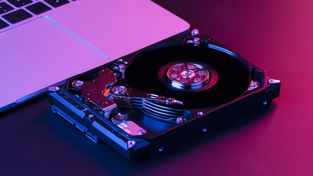
The modern smartphone—whether it’s the latest iPhone or a high-end Android device—is not just a communication tool; it’s a vault containing a person’s entire digital life. It is also an unparalleled forensic challenge. Thanks to advancements like Secure Boot processes and hardware-level encryption, when a mobile device suffers catastrophic physical damage (e.g., from a car crash, fire, or severe impact), the data, while still physically present on the memory chip, is locked away forever from standard recovery methods.
Retrieving data from such a device moves beyond simple repair and into the realm of digital forensics. It requires specialized, invasive techniques—primarily Chip-Off and In-System Programming (ISP)—to bypass the layers of security designed to prevent exactly this type of access. This surgical approach is mandatory for high-stakes scenarios like criminal investigations, litigation hold, or retrieving critical evidence when the device’s logic board is shattered.
The Digital Fortress: Why Mobile Data is Locked Down
Before attempting recovery, forensic specialists must contend with three immutable design features that make mobile data loss so absolute after physical trauma:
1. Soldered Memory (eMMC and UFS)
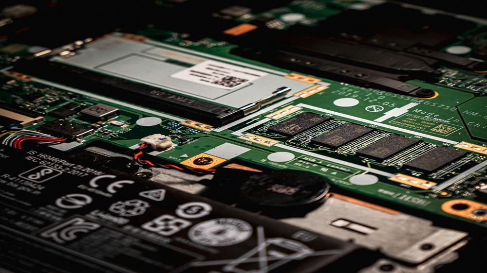
Modern smartphones no longer use easily removable storage cards. All data is stored on high-density eMMC (embedded MultiMediaCard) or UFS (Universal Flash Storage) memory chips that are soldered directly onto the main logic board using tiny Ball Grid Array (BGA) connections. If the logic board is cracked or shorted, the path to the memory is severed.
2. Secure Boot and TEE
The device relies on a chain of trust known as Secure Boot. When the device powers on, it verifies every component’s signature, including the operating system’s kernel. The decryption key required to access the data is often stored within the device’s Trusted Execution Environment (TEE), a highly protected zone of the processor. If the device cannot complete its secure boot sequence due to physical damage to the CPU or TEE (even if the memory chip is intact), the key is never released, and the data remains encrypted. To learn more about how the Trusted Execution Environment works, you can consult technical white papers on ARM’s security architecture.
3. Hardware-Bound Encryption
Unlike older devices where encryption was software-based, modern systems utilize hardware-bound encryption. The data is encrypted using keys that are intrinsically tied to the unique hardware identifiers and fuses burned into the device’s main CPU. Without the original, working CPU to perform the decryption on-the-fly, the raw data extracted from the memory chip is merely scrambled, unreadable binary code.
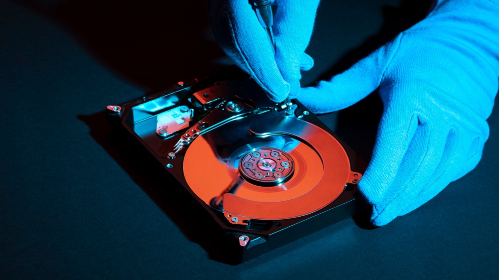
Forensic Strategy 1: Chip-Off Recovery (The Surgical Method)
The Chip-Off technique is the most aggressive and necessary method when the logic board is severely warped, cracked, or subjected to extreme environmental damage (fire, deep water).
The BGA Removal Process
-
Preparation and De-soldering: The damaged logic board is placed on a specialized BGA rework station. Using controlled heat, infrared sensors, and precision tweezers, the forensic engineer carefully heats the area beneath the eMMC or UFS chip. The goal is to melt the microscopic solder balls connecting the chip to the board without overheating or destroying the sensitive NAND memory layers inside the chip.
-
Cleaning and Reballing: Once removed, the chip’s BGA contact points must be meticulously cleaned of residual solder. If the chip’s contacts were damaged, a process called reballing (applying a fresh array of new, tiny solder balls) may be necessary to ensure a perfect connection in the next step.
-
Raw Data Acquisition: The prepared memory chip is inserted into a specialized NAND reader or chip-off adapter. This adapter bypasses the CPU and secure boot mechanism, allowing the forensic workstation to extract the raw, unencrypted, and scrambled binary image of the entire memory contents.
Chip-Off is an irreversible process that requires extreme precision. Any mistake in temperature control or physical force can render the memory chip permanently unusable.
Forensic Strategy 2: ISP Recovery (The Electronic Bypass)
The In-System Programming (ISP) method is preferred when the logic board is physically intact but fails to boot (e.g., due to minor power component damage or firmware corruption). ISP is less invasive than Chip-Off.
JTAG and eMMC/UFS Pinouts
-
Targeting Test Points: Forensic examiners locate specific, tiny test points on the logic board that connect directly to the eMMC or UFS memory lines. These points, often hidden beneath shields or protective coatings, are the device’s original manufacturing or testing interfaces (sometimes utilizing JTAG standards).
-
Micro-Soldering Wires: Using ultra-fine wires and micro-soldering techniques, the technician solders connections to these specific eMMC/UFS data, command, and clock lines. This is akin to attaching a direct intravenous line to the memory chip.
-
Data Extraction via Adapter: The soldered wires are connected to an ISP adapter which communicates directly with the memory chip, bypassing the malfunctioning power system and the secure boot process controlled by the CPU. This technique allows for the non-destructive reading of the raw memory contents. Specialized ISP pinout diagrams are essential for this process, which can be found in forensic hardware documentation on memory communication standards.
ISP is quicker and less destructive, but it relies on the physical integrity of the memory chip’s connections and the local circuit traces.
The Ultimate Hurdle: Decrypting the Raw Binary Image
After successfully extracting the raw binary data (via Chip-Off or ISP), the job is only half done. The data is still protected by hardware-bound encryption.
The memory image obtained is scrambled. To decrypt it, the forensic engineer must understand the device’s cryptographic architecture:
-
Key Derivation: The device’s encryption key is often derived from the user’s password/PIN, combined with the unique hardware key from the CPU.
-
The Missing Link: Because the CPU is dead or bypassed, the key derivation process cannot happen. The raw image must be fed into specialized, proprietary forensic decryption tools that attempt to emulate the device’s original security process.
-
The Password Challenge: If the user’s passcode is unknown, the decryption tool must perform a brute-force attack against the key derivation function, a computationally intensive process that can take days or weeks even with high-performance equipment. For devices with strong anti-tampering measures, an incorrect password attempt may irreversibly damage the key.
This step highlights why mobile forensic data recovery is a niche field: it combines the surgical skill of BGA rework with the computational power and cryptographic knowledge needed to break or bypass the secure key. For those interested in the physical tools used in this process, resources detailing advanced micro-soldering equipment and applications are widely available.
Why Standard Recovery Fails: The Fatal Flaw
Standard data recovery services fail spectacularly when faced with physically damaged mobile devices for simple reasons:
-
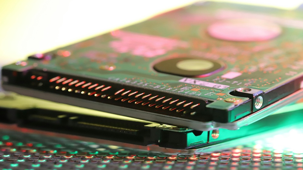
No Logic Board Swap: Unlike HDDs, the logic board cannot be swapped. The encryption key is tied to the original CPU. A new, working board will decrypt a new key, leaving the original data scrambled.
-
No Software Access: Recovery software cannot run because the device cannot complete its boot sequence and present a USB interface.
-
Irreversible Damage: Attempting to power on a liquid-damaged or cracked logic board can permanently short the memory chip, destroying the data that a specialized lab could have saved via Chip-Off.
For mobile devices with physical damage to the board, forensic Chip-Off and ISP are the final, non-negotiable options for data retrieval, used primarily when the data’s value—be it personal, corporate, or legal—outweighs the cost and complexity of the invasive procedure.
Conclusion: The Specialist is the Last Resort
When a smartphone is severely damaged, its military-grade security becomes its own executioner, locking the data inside a digital sarcophagus. The success of retrieving data from these devices depends entirely on the specialized skill of the recovery engineer to perform BGA Chip-Off, utilize ISP techniques, and overcome the cryptographic lock created by Secure Boot and hardware encryption.
If you have a physically damaged smartphone containing critical evidence or irreplaceable personal data, do not attempt to repair it or power it on. Contact DataCare Labs immediately to secure the device and initiate the specialized forensic recovery protocol.