Skip to content
 Forensic Recovery from NVMe and PCIe SSDs: The Challenge of High-Speed Interface Failures and Controller Loss

Introduction
The transition from the SATA interface to NVMe (Non-Volatile Memory Express) over the PCIe (Peripheral Component Interconnect Express) bus has delivered revolutionary speed to modern computing. NVMe SSDs are the gold standard for enterprise servers, high-end workstations, and gaming rigs, offering bandwidth up to 10 times faster than their SATA predecessors.
However, the architecture that delivers this speed—a complex, multi-lane communication protocol—also creates a unique, complex, and often catastrophic point of failure for data recovery specialists. When an NVMe drive dies, it does not fail like a simple plug-and-play device; it fails like a miniature, high-speed computer network.
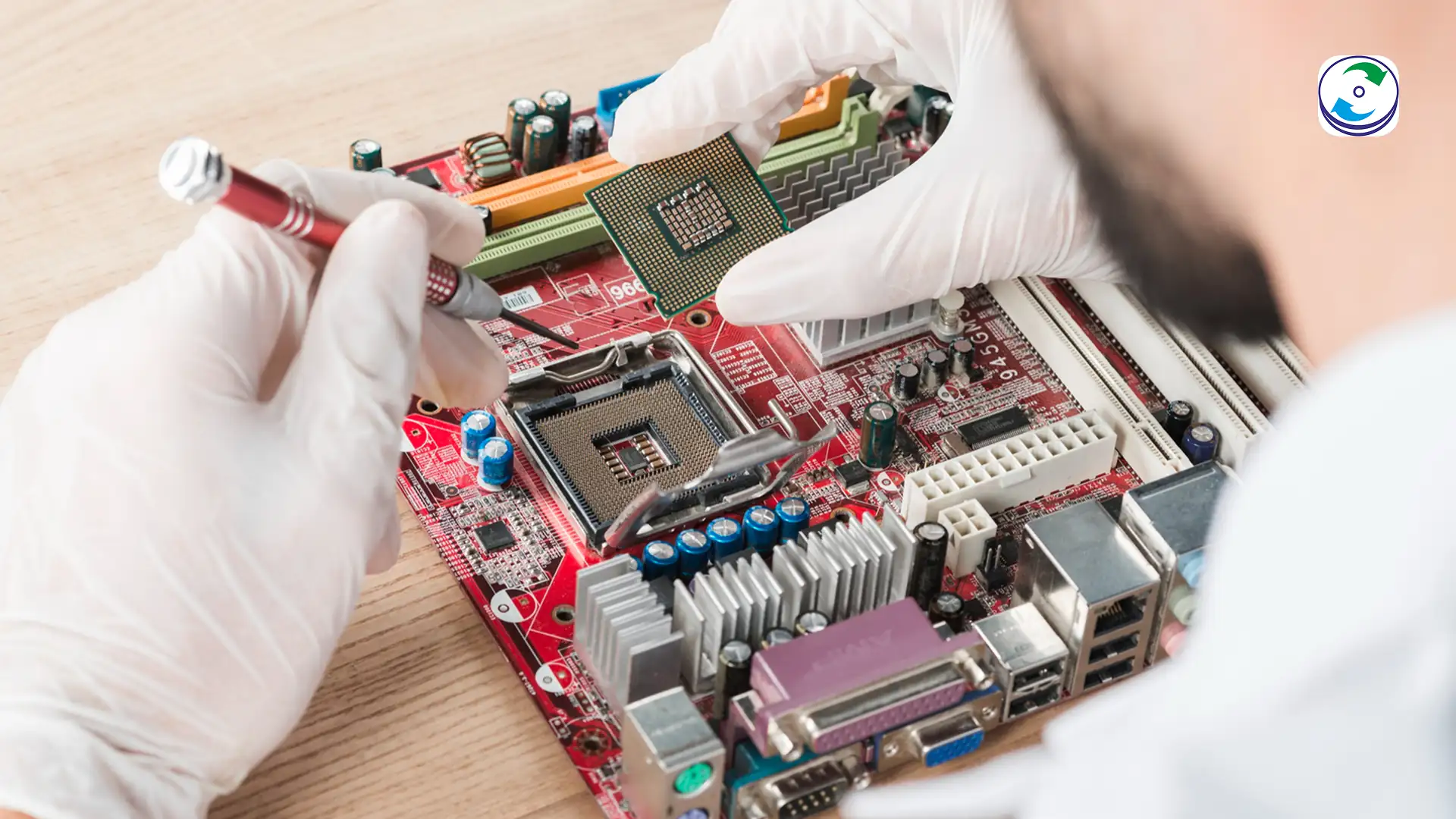
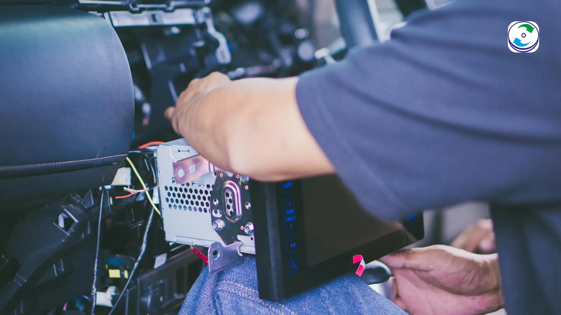
Recovering data from a failed NVMe drive is not just a job for a Cleanroom technician; it requires a specialized digital forensic engineer capable of performing intricate micro-soldering to revive a dead controller or perform a physical BGA chip-off extraction and then reverse-engineer a proprietary communication protocol. The complexity of NVMe recovery marks the cutting edge of data recovery science.
The NVMe Architecture: A Miniature Network of Failure
To understand the recovery challenge, one must first grasp the technological leap of the NVMe interface:
-
PCIe Bus Protocol: Unlike SATA, which funnels data through a single, slow queue, NVMe communicates directly with the CPU via multiple, high-speed PCIe lanes. This parallel communication vastly increases speed but also means the controller handles highly complex, simultaneous data streams.
-
Controller Dependence: The NVMe Controller (often branded by companies like Phison, Samsung, or Silicon Motion) is immensely powerful. It manages the complex mapping table (the physical location of every data bit) and handles the sophisticated hardware encryption that is mandatory for modern storage.
-
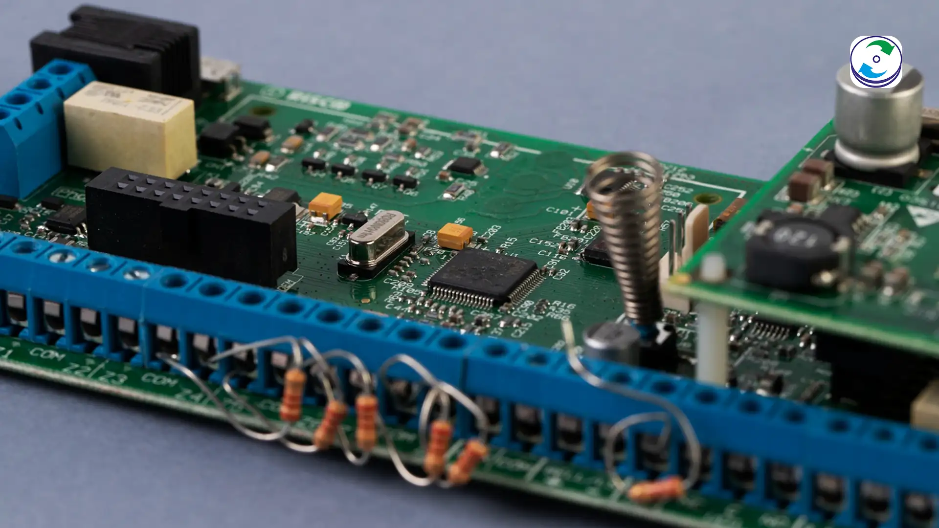
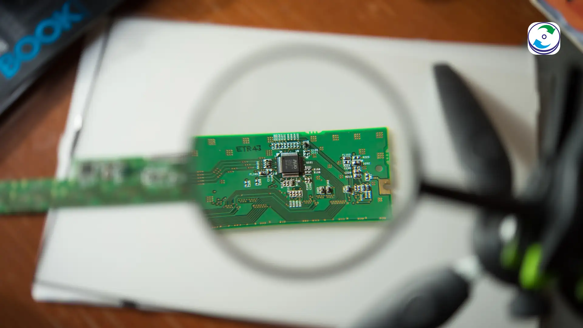
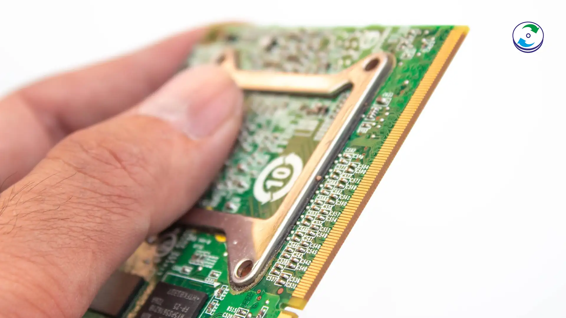
BGA NAND Chips: The actual data is stored on Ball Grid Array (BGA) NAND chips that are soldered directly onto the SSD circuit board. There are no easily removable components.
When the drive fails, the complexity of this architecture dictates that the failure is not isolated to a single component; it’s a systemic failure of the entire high-speed protocol.
The Two Catastrophic Failure Modes
NVMe drives typically succumb to one of two high-stakes failure modes, both of which eliminate standard recovery options.
Failure Mode 1: Electrical and Component Loss (Physical Death)
This is often caused by sudden power loss, voltage spikes, or overheating.
-
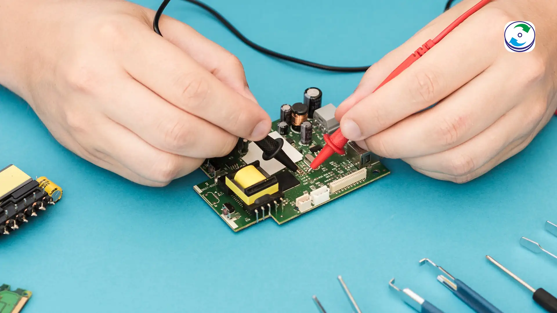
Targeting the Logic: Because the NVMe drive sits on the high-speed PCIe bus, electrical failure often targets the tiny power delivery components (fuses, capacitors, resistors) on the drive’s logic board. A short circuit here means the crucial controller chip cannot power up.
-
The Micro-Soldering Imperative: To recover the data, the drive’s controller—which holds the decryption keys and the mapping table—must be functional. Our engineers must perform micro-soldering repairs under high magnification to restore power to the controller, just enough to coax the drive into communicating its data before the failed component causes it to die again. Simply swapping the entire logic board is useless, as the controller’s unique firmware map is required to unscramble the data.
Failure Mode 2: Logical and Firmware Loss (Protocol Failure)
This occurs when the controller chip fails to correctly manage its complex internal data streams or firmware structure.
-
Controller Lockout: Firmware corruption can cause the controller to enter a protective, inaccessible state, often recognized by the host system as an unknown device or a drive with “0GB” capacity.
-
The Translation Barrier: Even if the NAND chips are physically healthy, the corruption of the translation layer (the map of where data is stored) means the controller cannot assemble the data correctly. The raw data stream is incomprehensible without the exact, proprietary ECC (Error Correction Code) and wear-leveling algorithm used by that specific controller model.
The Recovery Imperative: Bypassing the High-Speed Guard
For a dead NVMe drive, the recovery path must bypass the failed controller’s logic while accounting for the controller’s proprietary data scrambling.
Step A: BGA Chip-Off and Raw Data Acquisition
In cases where the logic board is too severely damaged for micro-soldering (e.g., severe liquid damage), we perform a BGA Chip-Off procedure:
-
De-soldering: Using precision infrared or hot-air rework stations, the tiny BGA NAND memory chips are delicately de-soldered from the PCB.
-
Raw Extraction: Each chip is mounted onto a specialized NAND reader, which extracts the raw, encrypted binary data. At this point, the data is a scrambled, unreadable jumble because it lacks the controller’s final processing.
Step B: Forensic Protocol Emulation
This is the most specialized and complex step, differentiating expert labs from the competition:
-
Algorithm Identification: The raw binary data is analyzed to identify the exact controller family (e.g., Phison E12, Samsung PM981).
-
Custom Decryptor Development: Forensic engineers use proprietary tools and extensive reverse-engineered knowledge to emulate the controller’s logic. They rebuild the exact mapping table and encryption sequence used by the failed controller in a safe, external environment.
-
Data Reassembly: This virtual emulation processes the raw, scrambled data, reassembling the pages, correcting errors, and decrypting the content into a coherent, readable file system image. This step is impossible without deep, specialized knowledge of NVMe proprietary protocols.
The DataCare Labs NVMe Protocol: Specialized Tools for High-Speed Media
DataCare Labs invests in the elite tools and training necessary to tackle the NVMe challenge:
-
Advanced Rework Stations: State-of-the-art BGA rework stations and microscopes are mandatory for the precision required to handle the microscopic components and chips of NVMe drives without causing thermal damage to the NAND flash.
-
Proprietary Chip-Off Tools: Specialized NAND readers and adapters are required for the hundreds of distinct models of BGA chips used in modern SSDs. No single, off-the-shelf tool can handle the entire range of NVMe chips.
-
Forensic Protocol Suites: We maintain and constantly update a library of reverse-engineered controller protocols to accurately emulate the specific mapping and encryption logic of major NVMe manufacturers, a capability that standard IT firms or general data recovery shops simply do not possess.
The complexity of NVMe failure means that DIY attempts are guaranteed to fail and likely cause irreversible damage to the sensitive NAND chips. When your high-speed drive goes dark, contact the specialists who understand the intricate physics and protocols of PCIe storage.